Plasma simulation for semiconductor fabrication
Understanding and simulating plasma is a key aspect of designing equipment to cost-effectively manufacture high-quality chips. Plasma simulation is essential to driving innovation in the semiconductor fabrication business.
This webinar covers fundamental physics and classifications using examples of plasma in the world around us. A range of plasma processes in semiconductor fabrication (such as plasma etching) is explored. A detailed focus is on the demonstration of plasma simulation within a wafer chamber using Simcenter STAR-CCM+ multiphysics software.
Sign up today to view this webinar and discover how the simulation of plasma processes is critical to efficient, high-quality manufacturing of chips for devices and systems we rely on today.
Harnessing plasma processes in the manufacture of high-quality semiconductors
Plasma, sometimes called “the forgotten state of matter”, is the most abundant state of matter in the universe. The sun, lightning bolts, the aurora borealis, and even the Orion Nebula are examples of natural plasma processes in action. In spite of this abundance, plasma physics remains somewhat of an enigma and a very active topic of research.
Plasma processes are common in semiconductor fabrication. The sand-to-silicon process is comprised of hundreds of steps, and many steps utilize plasma. Semiconductor and semiconductor equipment companies face ongoing and increasing challenges including chip miniaturization, manufacturing quality, and reliability requirements alongside competitive market pressures for efficient production. To address these, greater prediction and understanding of manufacturing equipment performance factors are important, especially those involving plasma processes such as plasma etching (dry and wet); deposition including sputtering; physical vapor deposition (PVD) or plasma-enhanced chemical vapor deposition (PECVD); coating; and plasma ashing.
How to apply multiphysics plasma simulation in semiconductor fabrication
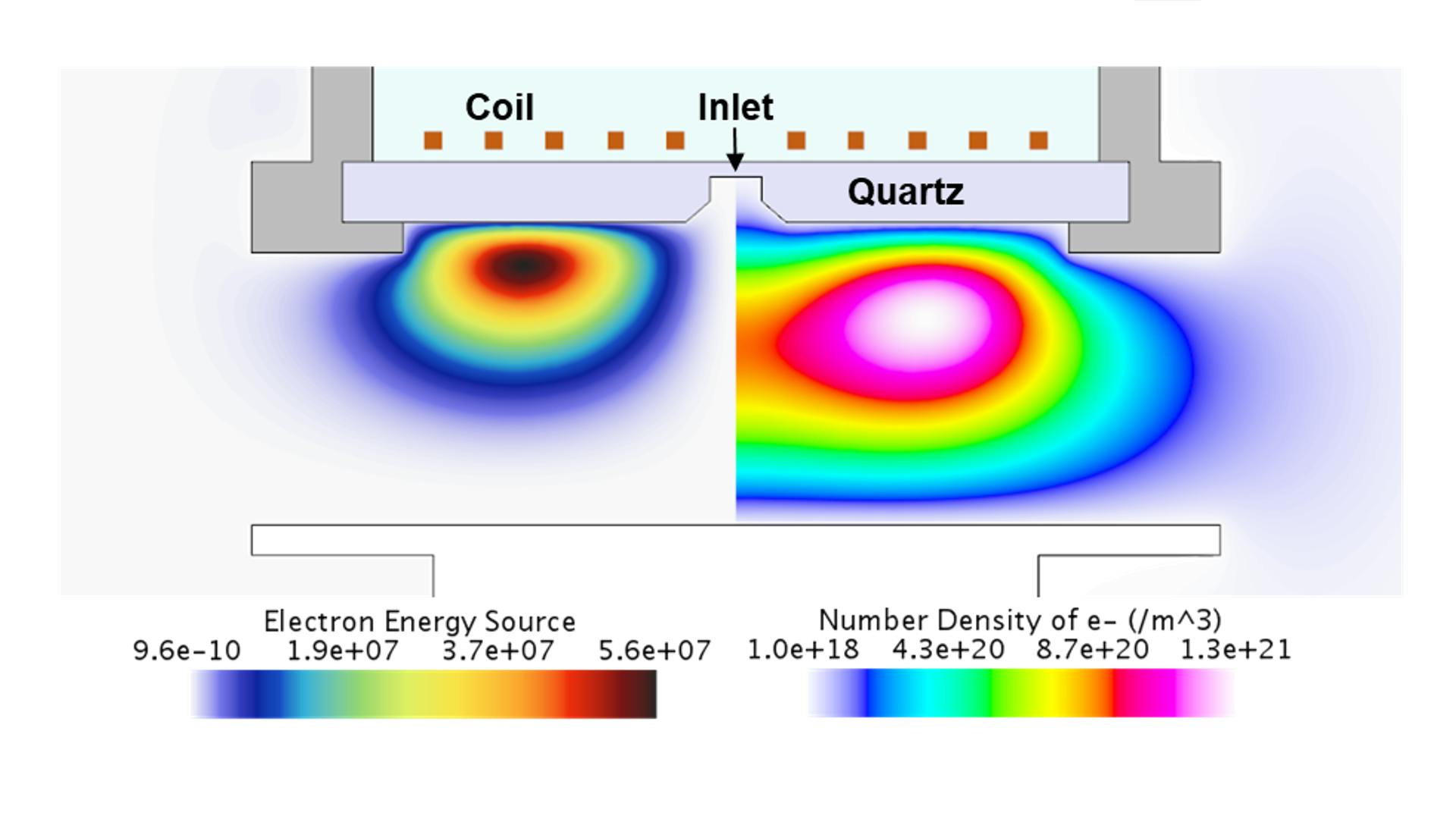
This presentation features a detailed description of a wafer chamber model in Simcenter STAR-CCM+ software for a study on factors influencing a plasma etch process. This includes an explanation of physics solvers and plasma chemistry applied, specification of chamber material properties, and electromagnetic coil performance, through to configuring of simulation criteria. Studies are performed to determine the level of Argon ion bombardment and to ensure a more homogenous ion bombardment across the wafer table surface to achieve the best etching rates.
Key results evaluated:
- Electron energy source and electron number density
- Electron temperature</li><li>Ion concentration and ion bombardment rates at table surface
Register to view this on-demand webinar if you are active in the development of a semiconductor manufacturing process involving plasma or in the design of semiconductor equipment to learn how to apply multiphysics simulation software to model a plasma process.